Thin Film Capacitors (MLCC)
As the size of electronic devices keep reducing, capacitors which have the small size, high precision and high capacitance become necessary. Thin film capacitor is one of the capacitors which satisfy above conditions. In our lab, we are focusing on MLCC and high-k which are the applications of thin film capacitors. MLCC, multi layer ceramic capacitor, is a small size capacitor which has a high capacitance with stacking thin film ceramics between electrodes. High-k is used for gate dielectric instead of silicon dioxide in miniaturizing MOSFET to increase gate capacitance without leakage current. For further development, we try to find out the detailed mechanism and characteristics with various experimental conditions. In MLCC case, degradation effect is the severe problem in this industry. In high-K capacitors, reduced dielectric constant by metal interface is major problem of this device.
However, it is difficult to investigate the detailed mechanism due to lack of knowledge in atomic scale level. In our lab, atomic scale EDS analysis is done to understand dopant distribution. In addition, in-situ biasing experiment is done to measure modulation of ionic polarization by applied voltage. Domain structure modulation can be described in atomic scale by this kind of in-situ experiment.
In case of high-K capacitors, E-field mapping by in-situ biasing experiment is done. During this process, charge distribution is measured by phase contrast(inline holography) technique and ionic charge is also measured by Electron Energy Loss Spectroscopy(EELS) technique. In addition, the electric field induced at the insulator is measured by 4D STEM technique which has high resolution(sub-nm scale) and sensitivity(0.4 MV/cm)

Next Generation Display (Quantum Dots)
Quantum dots (QD) are semiconductor nanocrystals, which exhibit quantum mechanical behavior arising from the specific size of their energy band gaps. Due to these properties, QDs find applications in a wide variety of electronics like solar cells, transistors, LEDs, medical imaging, and quantum computing. Chemistry lies at the core of modern industry and technology owing to its precise atomic and molecular control of reaction pathways. This has been particularly successful in the precise control of molecular structures for their specific purpose. The comprehensive resolution of such reaction pathways in terms of the reactants, intermediates, transition states, and products enables the development of new methods to create appropriate organic structures and materials. To unraveling the reaction pathways in full detail, TEM build a bridge towards atomic scale understanding of the structure and reaction. We are developing low dose imaging technique to overcome obstacles from the strong E-beam damage which degrades the nano structure we pursuit.

Next Generation Display – Nanowire LED
For last decades, Group III-N based Light Emitting Didoes, specially for InGaN, has been developed to actualize Red, Blue and Green my controlling the amount of InN. But, due to their lattice mismatch between InN and GaN, there exists inherent strain, defect, and strain-induced E-Field. By understanding the origin of those phenomena using state-of-art TEM can be a powerful tool to understand the device in atomic scale. and by combining in-situ electrical biasing in TEM, we can approach and solving the problem in device operation condition. Here, by taking the InGaN based planar & nanorod LED as a model system, we mapped the strain distribution with high resolution. And utilizing 4D-STEM, we are trying to map the Piezoelectric Field distribution in LED. Our technique will give inspiration to human to design the next-generation LED material and devices.

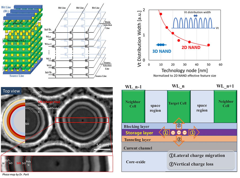
Next Generation Memory (V-NAND)
In order to increase data storage capacity in conventional memory devices, the size of individual devices has been reduced. However, as the size drops to the nanometer scale, data corruption due to interference between devices have become a critical issue. As a solution, multi-level-cell (MLC) and vertical stacking called VNAND instead of reducing the size in the lateral direction have been developed and it is currently commercialized. When the charge is stored in a layer called a charge trap layer (or floating gate), the threshold voltage changes. Maintaining the amount and distribution of charges constant is an important in determining the stability of the device since the threshold voltage varies according to the number of charges to be trapped. In this regard, characterizing the distribution of trapped charge in real devices can play an important role in revealing the cause of degradation of device performance. While excellent sensitivity and spatial resolution are required for it, there is no tool capable of imaging the charge distribution inside the device with existing measurement methods, and it relies on prediction by simulation. To characterize the charge distribution in VNAND device, we will carry out in-situ biasing inside a TEM combining phase imaging techniques to trace the trapped electrons at sub-nanometer scale.